Huawei Kirin 990 5G Review: Learn About Differences Between 7nm and 7nm+
In 2019, the International Consumer Electronics Show (IFA2019) was opened in Berlin, Germany. As we expected, Huawei held a new product launch today at IFA2019, launching the latest products of its own Kirin chip series, namely the Kirin 990 and Kirin 990 5G. Among them, most of the specifications of the world’s first flagship 5G SoC – Kirin 990 5G and Kirin 990 are the same. In addition to 5G support, there is only a small difference between the two.

Huawei Kirin 990 Parameters
The Kirin 990 5G is the world’s first flagship 5G SoC launched by Huawei. It is the industry’s smallest 5G mobile chip solution. Based on the industry’s most advanced 7nm+ EUV process, the 5G modem is integrated into the SoC for the first time. It is the first to support the NSA/SA dual architecture and TDD/FDD full frequency band. Based on the excellent 5G connection capability of the Baron 5000, the Kirin 990 5G achieves a leading 2.3Gbps peak download rate in the Sub-6GHz band with an upstream peak rate of 1.25Gbps.
This chip is the first flagship SoC with DaVinci architecture NPU. Its innovative design of NPU big core + NPU micro-core architecture is ideal for superior performance and energy efficiency for large computing scenarios. As for the CPU, the Kirin 990 uses a three-core energy-efficient architecture with two large cores + two medium cores and four small cores, with a maximum frequency of 2.86 GHz. The GPU is equipped with a 16-core Mali-G76. The new system-level Smart Cache implements intelligent offloading, which saves bandwidth and reduces power consumption.
In terms of gaming, the Kirin 990 5G is updated to Kirin Gaming+ 2.0 to achieve efficient collaboration of hardware foundations and solutions. In terms of photography, the Kirin 990 5G adopts the new ISP 5.0, and supports the BM3D (Block-Matching and 3D filtering) single-reverse hardware noise reduction technology on the mobile chip for the first time. As a result, the dark-light scene is brighter and clearer. Moreover, this chip comes with the world’s first dual-domain joint video noise reduction technology. The video noise processing is more precise, the video shooting is free from fear of dark scenes. The real-time video post-processing rendering technology is based on AI segmentation. The video picture adjusts the color frame by frame, and the smartphone video presents the film texture. HiAI Open Architecture 2.0 has been upgraded again. The framework and operator compatibility have reached the highest level in the industry. The number of operators is up to 300+. It supports all the mainstream framework models in the industry, providing developers with a more powerful and complete toolchain and enabling AI application development.
What Advantages Does It bring?
Looking back at the basic specifications of the Kirin 990 series chip, you will find that the first important technical point of the Kirin 990 5G is the process technology using a new generation of 7nm+ EUV lithography. Indeed, for a chip, its process is often the first concern of fans. So what does the 7nm+ process node used by the Kirin 990 5G mean? What is the so-called EUV lithography technology? Let’s dig deeper.
We believe you still remember that the Kirin 980 released last year is the world’s first mobile chip using 7nm process technology. After that, 7nm becomes the standard of the flagship mobile chip. But in fact, the 7nm chip we have used on the smartphone does not use a complete 7nm process, or it does not completely release the 7nm advantage. That’s why we call it the first generation 7nm process, and 7nm+ is the second generation 7nm process.
In May of this year, the news concerning to the 7nm+ process mass production has been leaked. This is the first time that the mobile processor goes to a mass-production using the EUV lithography technology. This made Intel and Samsung lead in the industry.
Obviously, the Huawei Kirin 990 5G is the first batch of mobile SoC using the 7nm+ process technology. So what does this 7nm+ process mean? What is the difference between it and the first generation 7nm process technology?
First of all, we have to understand the difficulty of the 7nm process node.
We know that the chip is made up of a large number of transistors. The transistor is also the most basic level of the chip. The conduction and truncation of each transistor represent 0 and 1. And even millions of transistors represent tens of millions or even hundreds of millions of 1 or 0. This is the basic principle of chip computing. Each transistor is very small.
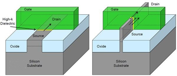
In the transistor structure, ‘Gate’ is mainly responsible for controlling the on and off of Source and Drain at both ends, and current flows from the source to the drain. At this time, the width of the gate determines the loss when the current passes, and the heat and power consumption are expressed. The narrower the width, the lower the power consumption. The width of the gate (gate length) is the value in the XX nm process.
For chip manufacturers, it is natural to strive for a narrower gate width. But when the width approaches 20 nm, the gate-to-current control capability drops sharply, the leakage rate increases accordingly, and the difficulty of the production process is also on the rise. However, as you know, this problem has been solved and it is not expanded here. And when the process continues to shrink, the difficulty will be further increased. People find that the original solution doesn’t work and brought another trick. Therefore, at the beginning of the 10nm node, chip manufacturers met difficulties in the production phase.
When the transistor size process is further reduced, less than 10 nm, quantum effects will occur. This is what we call the physical limit. The characteristics of the transistor will become difficult to control. At this time, the manufacturing difficulty of the chip is obviously exponentially increasing. It’s not only a technically difficulty but it also requires a lot of capital investment.
So what is the improvement in the two generations of technology from 7nm to 7nm+?
From the above introduction, we understood that with the continuous advancement of the chip process, the difficulty of chip manufacturing has also increased exponentially. Specific to the process of chip manufacturing, there is one of the most important processes, development and etching.
As you can see, light is projected through a mask (also called a reticle) with an integrated circuit pattern onto the photoresist-coated wafer to form an exposed and unexposed ‘pattern’. It is then etched away by a lithography machine.
This is just an explanation of the image. The actual process is extremely complicated. But what we need to know is that the choice of light source in this process is very important. The choice of the light source is actually the wavelength of the selected light. The shorter the wavelength, the smaller the actual size that can be exposed.
Prior to this, the most advanced was deep ultraviolet lithography (DUV), which is also an excimer laser, including KrF excimer laser (wavelength of 248 nm), and ArF excimer laser (wavelength of 193 nm). More advanced than DUV is EUV, which stands for extremely ultraviolet light.
Extreme ultraviolet lithography has a wavelength of up to 13.5 nm. The leap is very obvious. It is obviously more suitable for the manufacturing process of 7nm chips, which can greatly increase the density of transistors and reduce power consumption. Huawei said that the overall area of the Kirin 990 chip has not changed compared to the 980. But the number of transistors included has been greatly increased, reaching an astonishing 10.3 billion transistors. Thus, this is the first mobile chip with more than 10 billion transistors. Apart from this, it is clearly related to the adoption of the 7nm+ process technology. The increase in the number of transistors means an increase in chip processing power. Compared to the traditional 7nm process, the Kirin 990 series has a transistor density increase by 18%, energy efficiency increased by 10%, and AI operation will save more power.
In addition, the production of 7nm chips is not only EUV, but the advantages of EUV lithography are more obvious. DUV can also be used to produce 7nm chips. Last year’s first 7nm chips were still used in DUV lithography.
Therefore, the use of EUV lithography is also the key to distinguishing the second-generation 7nm process from the first generation. But this technology is very difficult to use. And there are many difficulties to be solved. For example, the EUV lithography machine has a light efficiency of only about 2%. And the active power is only 250W, which cannot meet the purpose of efficiently etching the wafer. In addition, the air molecules also interfere with the EUV light. So the vacuum environment is required for EUV lithography. In order to solve the mass production of 7nm+ process, Huawei has invested in a large number of process experts for research and development, with more than 5,000 verifications and a large number of experiments. The focus of it is obviously to solve the application of EUV lithography technology difficulties.
Of course, as a result, we already know that the 7nm+ process technology has been successfully mass-produced. The Kirin 990 also used this advanced technology for the first time – note that this is commercial, and the Huawei Mate 30 series smartphone will be released on September 19.
Undoubtedly, with the release of the Kirin 990 5G chip, the 7nm+ process will be the mainstream process technology standard for the mobile flagship chip, just like the 7nm process led by Kirin 980 last year.